DIL/NetPC DNP/1486
In-deep More Details
UART Sample
Contact us
Sales
Support
Back to Top Page
DIL/NetPC DNP/1486-3V: I/O Expansion Bus
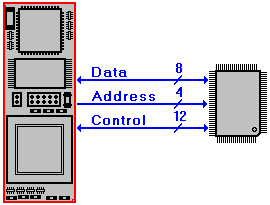
For the interface to external I/O devices, the DIL/NetPC DNP/1486-3V offers the I/O Expansion Bus signals. This bus consist of 8 data bits, 4 address bits and 12 control signals. The control signals are 4 programmable chip select outputs, 5 programmable interrupt inputs, I/O Read, I/O Write and a I/O Channel Ready signal.

With the I/O Expansion Bus the DIL/NetPC DNP/1486-3V can drive external devices, for example A/D- oder D/A- converters. Also LCDs (Text- or Small-Graphic modules) can be connected mostly directly with the I/O Expansion Bus signals without any glue-logic. The following table supplies a view to all signals of the I/O Expansion Bus.
J1 64-pin DIL Connector I/O Expansion Bus Signals
Pin
Name
Group
Function
Direction
40
INT5
Control
Programmable Interrupt Input 5
IN
41
INT4
Control
Programmable Interrupt Input 4
IN
42
INT3
Control
Programmable Interrupt Input 3
IN
43
INT2
Control
Programmable Interrupt Input 2
IN
44
INT1
Control
Programmable Interrupt Input 1
IN
45
CS4
Control
Programmable Chip Select Output 4
OUT
46
CS3
Control
Programmable Chip Select Output 3
OUT
47
CS2
Control
Programmable Chip Select Output 2
OUT
48
CS1
Control
Programmable Chip Select Output 1
OUT
49
IOCHRDY
Control
I/O Channel Ready
IN
50
IOR
Control
I/O Read Signal, I/O Expansion Bus
OUT
51
IOW
Control
I/O Write Signal, I/O Expansion Bus
OUT
52
SA3
Address
I/O Expansion Bus, Address Bit 3
OUT
53
SA2
Address
I/O Expansion Bus, Address Bit 2
OUT
54
SA1
Address
I/O Expansion Bus, Address Bit 1
OUT
55
SA0
Address
I/O Expansion Bus, Address Bit 0
OUT
56
SD7
Data
I/O Expansion Bus, Data Bit 7
IN/OUT
57
SD6
Data
I/O Expansion Bus, Data Bit 6
IN/OUT
58
SD5
Data
I/O Expansion Bus, Data Bit 5
IN/OUT
59
SD4
Data
I/O Expansion Bus, Data Bit 4
IN/OUT
60
SD3
Data
I/O Expansion Bus, Data Bit 3
IN/OUT
61
SD2
Data
I/O Expansion Bus, Data Bit 2
IN/OUT
62
SD1
Data
I/O Expansion Bus, Data Bit 1
IN/OUT
63
SD0
Data
I/O Expansion Bus, Data Bit 0
IN/OUT
The individual signals at this bus allow a very simple interface to external components. It is to be considered, however, that the DIL/NetPC DNP/1486-3V is a 3.3 volt-based system. The output levels are derived from the 3.3 volt supply voltage.
All inputs of the DIL/NetPC DNP/1486-3V I/O Expansion Bus can be driven by external 5 volt components. With other words: The inputs of the I/O Expansion Bus are 5 volt tolerant. Please absolutely note that this does not apply to all input pins of the DIL/NetPC DNP/1486-3V.
The 8-bit data SD7...SD0 is available at the I/O Expansion Bus with the Pins 56 - 63. The Pins 52 - 55 are four address bits SA3 ... SA0. Please consider, that a DIL/NetPC DNP/1486-3V-based system don´t need external address decoders for chip select generation to external components. With the pins 45 - 48 the DIL/NetPC DNP/1486-3V offers four programmable chip select signals CS4 ... CS1. The four address lines are used therefore only for the internal register selection in external devices.
![]()
DIL/NetPC DNP/1486-3V: Read/Write Timing of the I/O Expansion Bus
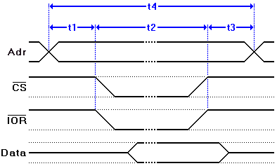
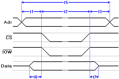
For the activation of I/O Expansion Bus Read/Write cycles the DIL/NetPC DNP/1486-3V has the signals IOR (I/O Read, pin 50, low activ) and IOW (I/O Write, pin 51, low activ). The timing of one Read/Write bus cycle can be influenced about IOCHRDY at the pin 49.

Figure 1: Read Timing of the I/O Expansion Bus
For external interrupts to the DIL/NetPC DNP/1486-3V, stand at the pins 40 ... 44 the programmable interrupt inputs INT5 to INT1 for the disposal. The figure 1 shows clearly the timing with the read access (I/O Expansion Bus Read Cycle) on external I/O devices. Figure 2 includes the same information for the write access (I/O Expansion Bus Write Cycle).

Figure 2: Write Timing of the I/O Expansion Bus
The following table includes the timing values for the individual times of the figure 1 (I/O Expansion Bus Read Cycle) and figure 2 (I/O Expansion Bus Write Cycle). All values are to be considered as "typical". The entire timing for write and read accesses at the I/O Expansion Bus of a DIL/NetPC DNP/1486-3V is in approximately compatible to the ISA bus.
Timing Values for Read/Write Cycles in Figure 1 and 2
Symbol
Parameter
Typ.
Units
t1
Address Prefetch Time
360
nsec.
t2
Chip Select Pulse Width
540
nsec.
t3
Address Hold Time
330
nsec.
t4
Read Cycle Time
1230
nsec.
t5
Write Cycle Time
1350
nsec.
t6
Data Prefetch Time
300
nsec.
t7
Data Hold Time
100
nsec.
SSV EMBEDDED SYSTEMS. Board Level Products. File: dnp0006.htm, Last Update: 07.Jan.2012
Copyight (c) 1996 - 2012 SSV and KDW. All rights reserved. webmaster@ist1.de